Tuesday, February 12, 2013

Picking Dies Off of Dicing Tape

Typically providers of dicing tape provide a specification sheet on material but rarely does it include any information on pick force required to remove the die from the tape.  In a Journal of Solid Mechanics and Material Engineering article in 2010 LINTEC Corporation published a study of pick force versus peel strength.  In it a way to approximate pick force required was introduced.

Study on Peeling Behavior

Formula for Determining Pick Force Required

The study concluded that there was a correlation, but the study focused on die attached adhesives in sheet format not in dicing tapes themselves.  It does beg the question though can dicing tape pick force be determined by peel strength.  While this paper provides no definitive answer I may be able to comment on this in a future posting. 

Friday, February 8, 2013

Laser Dicing

Laser Dicing is reported to have a number of advantages over blade dicing.

Advantages:
     - Faster cutting speed versus blade dicing
     - Less Backside Chipping
     - Narrower Kerf (Distance between chips(dies))
             o More product per wafer
     - Many laser singulation technologies do not use water

Laser Dicing Singulation of Silicon
Stealth Dicing Article
Chip Scale Review Article (pg.26)

What is often overlooked is the role of dicing tape in laser dicing.  Laser dicing produces considerably more heat than a blade dicing process.  This is one of the reasons why Synova developed the waterjet full ablation laser dicing system.

Traditional dicing tapes will heat and melt under the temperature generated by the laser and each type of laser dicer requires a different tape depending on the process.
      
Waterjet Laser Dicing: Porous tape or high adhesion tape.

Full Ablation (Full-Cut) Dicing: Tape which can withstand the energy generated by the laser.

Stealth Dicing: Expandable tape (frontside stealth dicing) or a transparent one for stealth dicing from the backside.

The advantages of laser dicing are compelling; lower CoO through faster throughput, more devices per wafer, and potentially increased die strength, but one must not neglect the role dicing tape plays in this process as laser dicers need to be paired with the right tape to work well.

If you have questions please leave a comment.

Tuesday, February 5, 2013

Scribe and Break Process

There are many varying singulation technologies available and while on the surface singulation of wafers seems straight forward achieving singulation with minimal backside chipping can be quite challenging.  As previously noted Dice Before Grind can be used to minimize backside chipping and improve die strength versus the industry standard blade dicing, but other techniques are available and can make sense depending on the device being singulated.

Scribe and Break is a process that does not rely on cutting through the wafer but creating either an internal fracture in the case of Laser Stealth Dicing or dicing a few microns into the top side with a blade or a laser and using an expansion process to expand the wafer so that in breaks along the scribed line or use an anvil to create the same result.  Below is an article on the process.


Critical to the success of this process is the tape.  The tape itself requires even expansion for two purposes.  The first is to allow the dies to singulate.  The second is to allow the kerf width (distance between dies) to be consistent in both X and Y directions for subsequent processing.  The link below can help recommend a dicing tape for a scribe and break process.


If you have any questions then please feel free to post questions below.

UV Dicing Tape Scribe and Break Tape


Friday, February 1, 2013

TAIKO Process. Is it viable for TSV production?

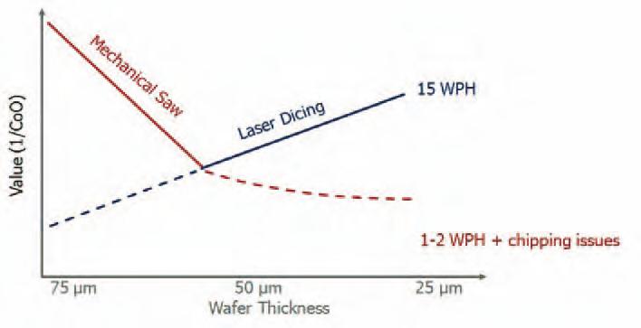
TAIKO is a process where a thick wafer is thinned in the center to allow backside development. 


The semiconductor industry is facing a major challenge to increase the speed of certain core technologies without increasing costs to consumers.  At the Flash Memory Conference last year one of the topics was on achieving higher speeds for DRAM in order to support next generation technologies.  The problem is the speed limits of wire bonding have been reached and subsequent technology improvements will require the use of TSV (Through Silicon Vias).

The issue with TSV is one of yield and cost.  The biggest issue today is how to handle thin ground wafers in order to develop the trenchs and backside connection points needed to enable a stack of DRAM dies using TSV.  The common approach is to attach a support to the wafer and then thin the backside.  Every approach used to form the vias relies at some point on handling thinned wafers and the support is required in all process flows.  Debonding and removing the support is problematic which effects yield.  In addition the cost of the support materials is not cheap and adds increasing cost to devices that are marketed to end users that are cost sensitive.

A potential solution is the TAIKO process, but can the TAIKO process be used for TSV production?  The TAIKO process (illustrated below) has one major issue.  It does not protect the circuit side during processing.
Below is a link to a presentation for a way to overcome this issue potentially.
 
TSV H-WSS Alternative Carrier Less Processing

TSV Update Disco October 2012


On the left is a picture of a wafer coated with a protective substance and TAIKO ground.  With no carrier it does not require additional capital investment to remove a carrier or apply an expensive bonding material.  This could be the path forward to enable higher yield lower cost TSV.


Once TSV are formed with TAIKO wafer dicing tape mounter becomes critical.  The reason is the large lip makes it near impossible to mount the dicing tape to the wafer.  A new wafer mounter from LINTEC the RAD-2512F/12 can solve this issue.
LINTEC RAD-2512F/12

TAIKO TSV Wafer Mounter

If the new coating can resist the steps required for various backside development and be used in conjunction with a wafer mounter designed to mount tape to a TAIKO wafer it is possible TAIKO's lower CoO will help enable the next generation of devices.